“Understanding Wafers: The Heartbeat of Semiconductor Innovation.”
Introduction
Wafers are the foundational building blocks of semiconductor manufacturing, serving as the substrate upon which integrated circuits (ICs) are fabricated. These thin, circular slices of semiconductor material, typically silicon, undergo a complex series of processes including doping, etching, and layering to create the intricate electronic components that power modern technology. Understanding wafers is crucial for grasping the intricacies of semiconductor fabrication, as they play a pivotal role in determining the performance, efficiency, and scalability of electronic devices. This introduction delves into the significance of wafers in the semiconductor industry, exploring their properties, manufacturing processes, and the technological advancements that continue to shape this vital sector.
What Are Wafers and Their Role in Semiconductor Manufacturing
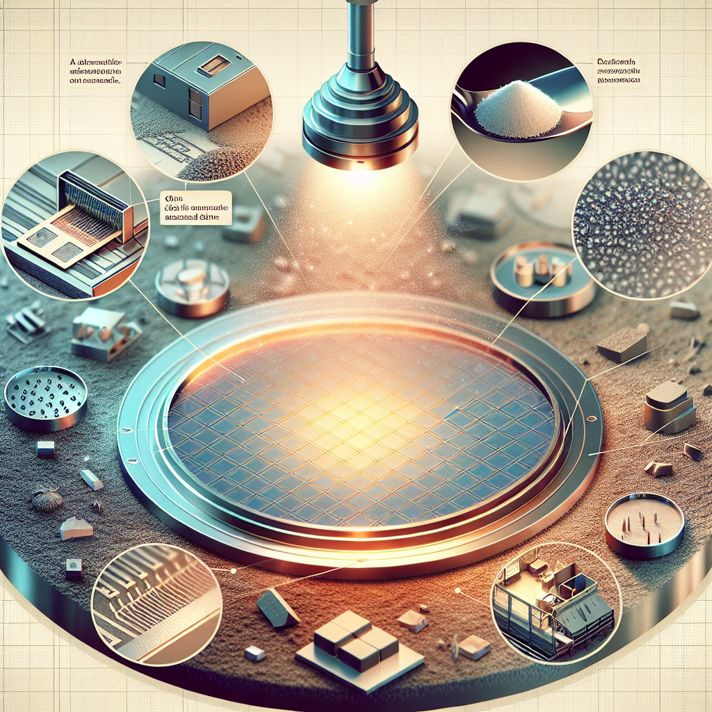
Wafers are thin, flat discs made from semiconductor materials, primarily silicon, and they serve as the foundational building blocks in the semiconductor manufacturing process. These wafers are typically sliced from a larger crystal, known as a boule, which is grown through processes such as the Czochralski method or the float-zone method. The purity and crystalline structure of the silicon used in wafers are critical, as they directly influence the performance and reliability of the semiconductor devices that will be fabricated on them.
Once the wafers are produced, they undergo a series of intricate processes that transform them into functional microelectronic components. The first step in this transformation is the cleaning of the wafers to remove any contaminants that could interfere with subsequent manufacturing steps. This is followed by the application of a photoresist layer, which is a light-sensitive material that allows for the precise patterning of circuits on the wafer surface. Photolithography, a key technique in semiconductor fabrication, utilizes ultraviolet light to transfer these patterns onto the wafer, enabling the creation of intricate circuit designs.
After the photolithography process, the wafers undergo etching, where unwanted material is removed to reveal the desired patterns. This step is crucial, as it defines the physical structure of the semiconductor devices. The etching process can be either wet or dry, depending on the specific requirements of the design and the materials involved. Following etching, various doping processes are employed to introduce impurities into the silicon, which alters its electrical properties and allows for the creation of p-type and n-type semiconductors. This doping is essential for forming the junctions that are fundamental to the operation of transistors and diodes.
As the manufacturing process continues, additional layers of materials are deposited onto the wafer through techniques such as chemical vapor deposition (CVD) or physical vapor deposition (PVD). These layers can include insulators, conductors, and other semiconductor materials, each serving a specific function in the overall device architecture. The careful control of thickness and composition during these deposition processes is vital, as even minor deviations can lead to significant performance issues in the final product.
Once all the necessary layers have been deposited and processed, the wafers undergo a series of tests to ensure that they meet the required specifications. This testing phase is critical, as it helps identify any defects or inconsistencies that could affect the performance of the semiconductor devices. After passing these tests, the wafers are then diced into individual chips, known as dies, which are subsequently packaged for integration into electronic systems.
In summary, wafers play an indispensable role in semiconductor manufacturing, serving as the substrate upon which complex electronic circuits are built. The processes involved in transforming a simple silicon wafer into a sophisticated microelectronic device are intricate and require precision at every stage. From the initial crystal growth to the final packaging of individual chips, each step is meticulously designed to ensure that the resulting devices meet the high standards of performance and reliability demanded by modern technology. As the demand for smaller, faster, and more efficient electronic devices continues to grow, the importance of wafers and the processes surrounding their manufacture will only become more pronounced in the ever-evolving landscape of semiconductor technology.
The Different Types of Wafers Used in the Industry
Wafers are fundamental components in the semiconductor manufacturing process, serving as the substrate upon which integrated circuits (ICs) are built. The type of wafer used can significantly influence the performance, efficiency, and cost of the final semiconductor device. In the industry, various types of wafers are employed, each tailored to specific applications and manufacturing requirements. Understanding these different types is crucial for anyone involved in semiconductor technology.
Silicon wafers are the most prevalent in the semiconductor industry, primarily due to silicon’s excellent electrical properties and abundance. These wafers are typically produced in diameters ranging from 100 mm to 300 mm, with 200 mm and 300 mm wafers being the most common in high-volume manufacturing. Silicon wafers can be further categorized into single-crystal and polycrystalline types. Single-crystal silicon wafers, often produced using the Czochralski process, exhibit superior electrical characteristics and are essential for high-performance applications. In contrast, polycrystalline silicon wafers, which consist of multiple silicon crystals, are generally used in less demanding applications, such as solar cells.
In addition to silicon, other materials are gaining traction in the semiconductor industry, particularly for specialized applications. Gallium arsenide (GaAs) wafers, for instance, are known for their high electron mobility and direct bandgap, making them ideal for high-frequency and optoelectronic devices, such as lasers and LEDs. GaAs wafers are typically more expensive than silicon wafers, but their unique properties justify the cost in applications where performance is paramount. Similarly, indium phosphide (InP) wafers are utilized in high-speed and high-frequency applications, particularly in telecommunications and fiber optics, due to their superior electron transport properties.
Another emerging category of wafers is silicon carbide (SiC) and gallium nitride (GaN) wafers, which are increasingly used in power electronics and high-temperature applications. SiC wafers are particularly valued for their ability to operate at higher voltages and temperatures compared to traditional silicon wafers. This makes them ideal for applications in electric vehicles and renewable energy systems, where efficiency and thermal management are critical. GaN wafers, on the other hand, are gaining popularity in RF and microwave applications due to their high breakdown voltage and efficiency, making them suitable for 5G technology and advanced radar systems.
Moreover, the advent of advanced packaging technologies has led to the development of wafer-level packaging (WLP), which allows for the integration of multiple functions within a single wafer. This approach not only reduces the size of the final product but also enhances performance by minimizing interconnect lengths. WLP can be applied to various types of wafers, including silicon and compound semiconductor wafers, further expanding the versatility of semiconductor manufacturing.
As the semiconductor industry continues to evolve, the demand for innovative materials and wafer types is likely to grow. Research and development efforts are focused on exploring new materials, such as two-dimensional materials and organic semiconductors, which could potentially revolutionize the industry. These advancements will not only enhance the performance of semiconductor devices but also contribute to the ongoing miniaturization and integration of electronic components.
In conclusion, the different types of wafers used in the semiconductor industry play a pivotal role in determining the performance and applicability of integrated circuits. From traditional silicon wafers to advanced materials like GaAs, SiC, and GaN, each type offers unique advantages tailored to specific applications. As technology progresses, the exploration of new materials and wafer technologies will undoubtedly shape the future landscape of semiconductor manufacturing.
The Wafer Fabrication Process Explained

The wafer fabrication process is a critical component of semiconductor manufacturing, serving as the foundation for the production of integrated circuits. This intricate process begins with the selection of a suitable substrate, typically a silicon wafer, which is chosen for its excellent electrical properties and availability. The wafers are usually circular and can vary in diameter, with 200mm and 300mm being the most common sizes in contemporary manufacturing. Once the wafers are prepared, they undergo a series of meticulously controlled steps that transform them into functional semiconductor devices.
Initially, the wafers are cleaned to remove any contaminants that could interfere with subsequent processes. This cleaning is essential, as even minute particles can lead to defects in the final product. Following this, the wafers are subjected to oxidation, where a thin layer of silicon dioxide is grown on the surface. This oxide layer serves multiple purposes, including acting as an insulator and providing a protective barrier during later processing steps.
Next, the process of photolithography comes into play, which is pivotal in defining the intricate patterns that will form the various components of the semiconductor device. During photolithography, a photosensitive material known as photoresist is applied to the wafer’s surface. The wafer is then exposed to ultraviolet light through a mask that contains the desired circuit pattern. The exposed areas of the photoresist undergo a chemical change, allowing for selective removal in the subsequent development step. This process creates a precise pattern on the wafer, which is essential for the accurate placement of electronic components.
Once the pattern is established, the next phase involves etching, where the exposed silicon dioxide is removed to reveal the underlying silicon. This step is crucial, as it allows for the creation of the various layers that will eventually form transistors and other circuit elements. There are two primary etching techniques: wet etching, which uses chemical solutions, and dry etching, which employs plasma to remove material. Each method has its advantages and is chosen based on the specific requirements of the design.
Following etching, the wafer undergoes doping, a process that introduces impurities into the silicon to modify its electrical properties. This step is essential for creating p-type and n-type regions within the semiconductor, which are necessary for the operation of transistors. The doping process can be accomplished through various methods, including ion implantation and diffusion, each offering different levels of precision and control.
As the fabrication process continues, additional layers of materials are deposited onto the wafer. Techniques such as chemical vapor deposition (CVD) and physical vapor deposition (PVD) are commonly employed to create these layers, which can include metals, dielectrics, and other semiconductors. Each layer is carefully engineered to fulfill specific functions within the device, such as interconnections or insulation.
Finally, after numerous cycles of photolithography, etching, doping, and deposition, the wafer reaches the end of its fabrication journey. The completed wafer is then tested for defects and performance before being diced into individual chips, which will ultimately be packaged and integrated into electronic devices. This comprehensive wafer fabrication process underscores the complexity and precision required in semiconductor manufacturing, highlighting the importance of each step in producing reliable and efficient electronic components. As technology continues to advance, the methods and materials used in wafer fabrication will evolve, further enhancing the capabilities of modern electronics.
Challenges in Wafer Production and Quality Control
The production of wafers, which serve as the foundational building blocks of semiconductor devices, is fraught with challenges that can significantly impact both yield and quality. As the demand for smaller, faster, and more efficient electronic devices continues to rise, the semiconductor industry faces increasing pressure to enhance wafer production processes while maintaining stringent quality control measures. One of the primary challenges in wafer production is the inherent complexity of the manufacturing process itself. The journey from raw silicon to a finished wafer involves multiple intricate steps, including crystal growth, slicing, polishing, and doping. Each of these stages presents unique challenges that can introduce defects, thereby compromising the integrity of the final product.
For instance, during the crystal growth phase, any fluctuations in temperature or impurities in the raw materials can lead to dislocations or inclusions within the silicon lattice. These defects can propagate through subsequent processing steps, ultimately affecting the electrical properties of the semiconductor devices fabricated on the wafers. Consequently, maintaining a controlled environment and ensuring the purity of materials are critical to minimizing defects during this initial stage. Furthermore, the slicing of silicon ingots into wafers must be executed with precision. The use of diamond wire saws has become prevalent due to their ability to produce thinner wafers with reduced kerf loss. However, this process can also introduce micro-cracks or surface roughness, which can adversely affect the performance of the devices.
Once the wafers are sliced, they undergo a polishing process to achieve the desired surface finish. This step is crucial, as any imperfections on the wafer surface can lead to issues during photolithography, where patterns are transferred onto the wafer for circuit fabrication. The challenge lies in balancing the need for a smooth surface with the potential for introducing additional defects during the polishing process. As such, manufacturers must employ advanced techniques and materials to optimize this stage while ensuring that the wafers meet the stringent specifications required for high-performance applications.
In addition to the physical challenges associated with wafer production, quality control remains a paramount concern. The semiconductor industry operates under a zero-defect philosophy, where even minor imperfections can lead to significant failures in electronic devices. To address this, manufacturers have implemented rigorous inspection and testing protocols throughout the production process. Techniques such as optical inspection, scanning electron microscopy, and atomic force microscopy are employed to detect defects at various stages. However, the sheer volume of wafers produced necessitates the use of automated systems to ensure efficiency and consistency in quality control.
Moreover, as technology advances and the industry shifts towards smaller nodes, the complexity of the devices being manufactured increases. This trend necessitates even more stringent quality control measures, as the tolerance for defects becomes increasingly narrow. The integration of artificial intelligence and machine learning into quality control processes is emerging as a promising solution, enabling manufacturers to predict potential defects and optimize production parameters in real-time.
In conclusion, the challenges in wafer production and quality control are multifaceted and require a comprehensive approach to ensure the successful fabrication of semiconductor devices. By addressing the complexities of the manufacturing process and implementing advanced inspection techniques, the industry can strive to meet the growing demands for high-quality wafers. As technology continues to evolve, ongoing innovation in production methodologies and quality assurance will be essential to overcoming these challenges and sustaining the growth of the semiconductor sector.
Future Trends in Wafer Technology and Semiconductor Innovation
As the semiconductor industry continues to evolve, the future of wafer technology stands at the forefront of innovation, driving advancements that will shape the next generation of electronic devices. The increasing demand for higher performance, energy efficiency, and miniaturization in consumer electronics, automotive applications, and industrial systems necessitates a reevaluation of existing wafer technologies. One of the most significant trends is the shift towards larger wafer sizes, which allows for more chips to be produced per wafer, thereby reducing manufacturing costs and increasing yield. The transition from 200mm to 300mm wafers has already been widely adopted, and research is underway to explore even larger sizes, such as 450mm. This shift not only enhances productivity but also aligns with the industry’s goal of achieving economies of scale.
In addition to size, the materials used in wafer production are also undergoing transformation. Traditional silicon wafers are being complemented by advanced materials such as silicon carbide (SiC) and gallium nitride (GaN). These materials offer superior electrical properties, enabling devices to operate at higher voltages and temperatures, which is particularly beneficial for power electronics and high-frequency applications. As the demand for electric vehicles and renewable energy solutions grows, the adoption of these wide-bandgap semiconductors is expected to accelerate, paving the way for more efficient energy conversion and management systems.
Moreover, the integration of advanced manufacturing techniques is revolutionizing wafer technology. Techniques such as atomic layer deposition (ALD) and extreme ultraviolet (EUV) lithography are becoming increasingly prevalent, allowing for the fabrication of smaller, more complex features on wafers. These innovations not only enhance the performance of semiconductor devices but also enable the development of new architectures, such as 3D stacking and chiplet designs. By stacking multiple layers of chips vertically, manufacturers can significantly increase performance while minimizing the footprint, which is crucial in an era where space is at a premium.
As we look to the future, the role of artificial intelligence (AI) and machine learning in wafer manufacturing cannot be overlooked. These technologies are being harnessed to optimize production processes, predict equipment failures, and enhance quality control. By analyzing vast amounts of data generated during manufacturing, AI algorithms can identify patterns and anomalies, leading to improved yield rates and reduced downtime. This integration of smart technologies not only streamlines operations but also contributes to the overall sustainability of semiconductor manufacturing by minimizing waste and energy consumption.
Furthermore, the ongoing miniaturization of semiconductor devices is driving research into new fabrication techniques and materials. The development of nanoscale transistors and quantum-dot technologies holds promise for creating even smaller and more efficient chips. As these technologies mature, they will enable the production of devices that are not only faster but also capable of performing complex computations with minimal power consumption.
In conclusion, the future of wafer technology and semiconductor innovation is poised for remarkable advancements. The combination of larger wafer sizes, the adoption of new materials, the integration of advanced manufacturing techniques, and the application of AI will collectively redefine the landscape of semiconductor manufacturing. As these trends continue to unfold, they will not only enhance the capabilities of electronic devices but also contribute to a more sustainable and efficient technological ecosystem. The semiconductor industry stands on the brink of a new era, one that promises to deliver unprecedented performance and innovation across a multitude of applications.
Q&A
1. **What is a wafer in semiconductor manufacturing?**
A wafer is a thin slice of semiconductor material, typically silicon, used as the substrate for fabricating integrated circuits and other microdevices.
2. **How are wafers produced?**
Wafers are produced through a process called crystal growth, where silicon is melted and then cooled to form a single crystal ingot, which is then sliced into thin discs.
3. **What is the significance of wafer size in manufacturing?**
Larger wafers allow for more chips to be fabricated simultaneously, increasing production efficiency and reducing costs per chip.
4. **What processes are performed on wafers during semiconductor manufacturing?**
Wafers undergo various processes including photolithography, etching, doping, and deposition to create the intricate patterns and structures needed for electronic components.
5. **What are the common materials used for wafers besides silicon?**
Besides silicon, other materials used for wafers include gallium arsenide (GaAs), silicon carbide (SiC), and indium phosphide (InP), each chosen for specific electronic properties.
Conclusion
Understanding wafers is essential in semiconductor manufacturing as they serve as the foundational substrate for integrated circuits. Wafers are meticulously crafted from silicon and undergo various processes, including doping, etching, and layering, to create complex electronic components. Mastery of wafer technology is crucial for optimizing performance, yield, and cost-effectiveness in the production of semiconductors, which are vital for modern electronics. As the demand for smaller, faster, and more efficient devices continues to grow, advancements in wafer fabrication techniques will play a pivotal role in the future of technology.