“Advanced Packaging: Pioneering the Future of Semiconductor Miniaturization.”
Introduction
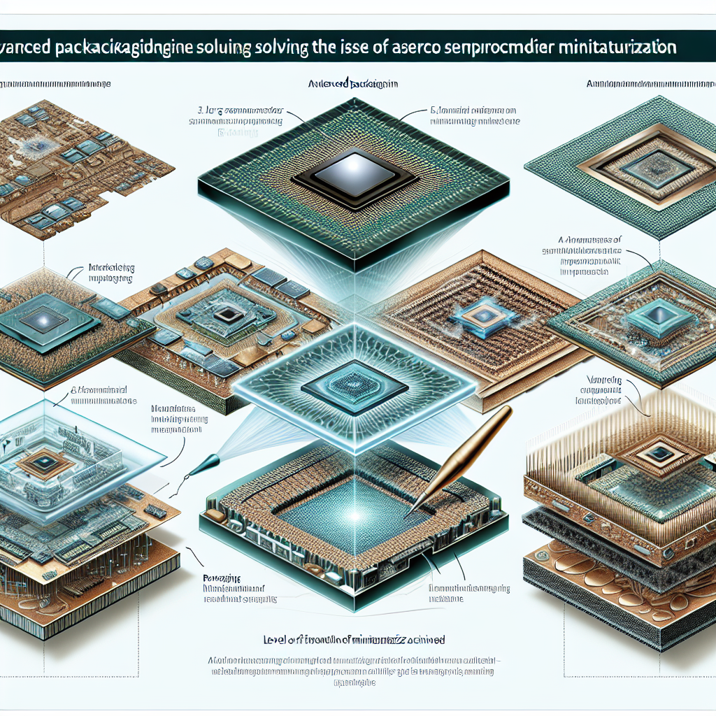
Advanced packaging technologies are playing a crucial role in addressing the challenges of semiconductor miniaturization. As the demand for smaller, more powerful electronic devices continues to rise, traditional scaling methods face limitations due to physical and thermal constraints. Advanced packaging techniques, such as 3D stacking, system-in-package (SiP), and chiplet architectures, enable the integration of multiple components into a compact form factor while enhancing performance and energy efficiency. These innovations not only facilitate the continued miniaturization of semiconductors but also improve signal integrity, reduce power consumption, and enable heterogeneous integration, ultimately driving the evolution of next-generation electronics.
Enhanced Thermal Management in Advanced Packaging
As semiconductor devices continue to shrink in size while increasing in functionality, the challenge of managing heat dissipation has become increasingly critical. Advanced packaging technologies are emerging as a vital solution to this issue, providing enhanced thermal management that is essential for maintaining performance and reliability in miniaturized electronic components. The miniaturization of semiconductors leads to higher power densities, which in turn generates more heat. If not effectively managed, this heat can lead to thermal runaway, reduced performance, and ultimately, device failure. Therefore, the integration of advanced packaging techniques is crucial for ensuring that these compact devices operate within safe thermal limits.
One of the primary methods employed in advanced packaging to enhance thermal management is the use of thermal interface materials (TIMs). These materials are strategically placed between the semiconductor die and the heat spreader or heat sink to improve thermal conductivity. By minimizing the thermal resistance at these interfaces, TIMs facilitate more efficient heat transfer away from the chip. Recent innovations in TIM formulations, including the development of phase change materials and high-conductivity composites, have significantly improved their performance, allowing for better thermal management in densely packed semiconductor assemblies.
In addition to TIMs, advanced packaging techniques such as 3D packaging and system-in-package (SiP) architectures are also playing a pivotal role in thermal management. These approaches allow for the vertical stacking of multiple semiconductor dies, which can lead to increased thermal coupling between layers. While this can pose challenges in terms of heat dissipation, it also opens up opportunities for innovative cooling solutions. For instance, microfluidic cooling systems can be integrated into the packaging design, enabling the circulation of coolant fluids that absorb heat more effectively than traditional air cooling methods. This not only enhances thermal performance but also allows for more compact designs, as the cooling system can be integrated directly into the package.
Moreover, the use of advanced materials in packaging is another key factor in improving thermal management. Materials such as silicon carbide (SiC) and gallium nitride (GaN) are increasingly being utilized due to their superior thermal conductivity and high-temperature performance. These materials not only help in dissipating heat more effectively but also contribute to the overall reliability of the semiconductor devices. By incorporating these advanced materials into the packaging design, manufacturers can create solutions that withstand higher operational temperatures, thereby extending the lifespan of the devices.
Furthermore, the implementation of thermal simulation tools during the design phase of semiconductor packaging has become essential. These tools allow engineers to model thermal behavior and predict potential hotspots within the package. By identifying areas of concern early in the design process, engineers can make informed decisions about material selection, layout, and cooling strategies. This proactive approach to thermal management not only enhances the performance of the final product but also reduces the risk of costly redesigns and delays.
In conclusion, as the semiconductor industry continues to push the boundaries of miniaturization, advanced packaging technologies are proving to be indispensable in addressing the challenges of thermal management. Through the use of innovative thermal interface materials, advanced packaging architectures, high-performance materials, and sophisticated simulation tools, manufacturers are able to effectively manage heat dissipation in compact devices. This not only ensures optimal performance and reliability but also paves the way for the next generation of high-performance electronics that meet the demands of an increasingly digital world.
3D Integration Techniques for Compact Designs
As the semiconductor industry continues to push the boundaries of miniaturization, advanced packaging techniques have emerged as a pivotal solution to meet the demands of compact designs. Among these techniques, 3D integration stands out as a transformative approach that not only enhances performance but also optimizes space utilization. By stacking multiple layers of semiconductor devices vertically, 3D integration allows for a significant reduction in footprint while maintaining or even improving functionality. This method is particularly advantageous in applications where space is at a premium, such as in mobile devices, wearables, and Internet of Things (IoT) devices.
One of the key advantages of 3D integration is its ability to reduce interconnect lengths. Traditional 2D designs often require extensive routing of signals across a larger surface area, which can introduce latency and increase power consumption. In contrast, 3D integration minimizes these distances by allowing direct vertical connections between layers. This not only enhances signal integrity but also contributes to lower power requirements, making it an attractive option for energy-sensitive applications. Furthermore, the reduction in interconnect length can lead to improved thermal performance, as heat dissipation can be more effectively managed in a compact structure.
Moreover, 3D integration techniques facilitate the integration of heterogeneous materials and functionalities. This capability allows designers to combine different types of chips—such as logic, memory, and sensors—into a single package. By leveraging various technologies, manufacturers can create systems that are not only smaller but also more powerful and versatile. For instance, integrating high-performance processors with memory stacks in a 3D configuration can significantly enhance data processing speeds while conserving space. This versatility is particularly beneficial in the rapidly evolving landscape of artificial intelligence and machine learning, where processing power and efficiency are paramount.
In addition to performance benefits, 3D integration also addresses the challenges associated with traditional scaling methods. As semiconductor nodes shrink, the physical limitations of materials and manufacturing processes become increasingly pronounced. 3D integration offers a way to circumvent some of these limitations by allowing for the stacking of chips rather than relying solely on lateral scaling. This approach not only extends the life of existing technologies but also opens the door to innovative designs that were previously unattainable.
Transitioning to 3D integration, however, is not without its challenges. The manufacturing processes involved are more complex than those used in traditional 2D designs. Techniques such as through-silicon vias (TSVs) and micro-bumps are essential for establishing electrical connections between layers, and these require precise fabrication and alignment. Additionally, thermal management becomes more critical in a 3D structure, as the increased density of components can lead to hotspots that must be effectively dissipated. Nevertheless, ongoing advancements in materials science and manufacturing technologies are steadily overcoming these hurdles, paving the way for broader adoption of 3D integration.
As the semiconductor industry continues to evolve, the importance of advanced packaging techniques like 3D integration cannot be overstated. By enabling compact designs that enhance performance and efficiency, these techniques are not only addressing the immediate challenges of miniaturization but are also setting the stage for future innovations. As we look ahead, it is clear that 3D integration will play a crucial role in shaping the next generation of semiconductor devices, driving progress in a wide array of applications and industries. In this context, the synergy between advanced packaging and semiconductor miniaturization will undoubtedly continue to redefine the landscape of technology.
Advanced Materials for Improved Performance

The relentless pursuit of miniaturization in semiconductor technology has necessitated the development of advanced materials that enhance performance while accommodating the shrinking dimensions of electronic components. As devices become smaller and more powerful, the materials used in semiconductor packaging must evolve to meet the increasing demands for efficiency, thermal management, and electrical performance. This evolution is critical, as traditional materials often fall short in addressing the challenges posed by modern applications, particularly in high-performance computing, telecommunications, and consumer electronics.
One of the most significant advancements in this area is the introduction of new dielectric materials that offer superior insulating properties. These materials are essential for reducing parasitic capacitance, which can hinder signal integrity and increase power consumption in densely packed circuits. For instance, low-k dielectrics have emerged as a solution to mitigate these issues, allowing for faster signal transmission and reduced power loss. By incorporating materials with lower dielectric constants, manufacturers can achieve higher performance levels while maintaining the compact form factors that modern devices require.
In addition to dielectric materials, the use of advanced thermal interface materials (TIMs) has become increasingly important in semiconductor packaging. As devices operate at higher speeds and generate more heat, effective thermal management is crucial to ensure reliability and longevity. Traditional thermal management solutions often struggle to dissipate heat efficiently, leading to performance degradation. However, innovative TIMs, such as those based on graphene or metal matrix composites, provide enhanced thermal conductivity, enabling better heat dissipation. This improvement not only enhances the performance of individual components but also contributes to the overall reliability of the system.
Moreover, the integration of advanced materials extends beyond just thermal and dielectric properties. The mechanical properties of packaging materials are equally vital, particularly as devices are subjected to various stresses during manufacturing and operation. Advanced polymers and composites are being developed to provide the necessary mechanical strength while remaining lightweight and flexible. These materials can withstand the rigors of thermal cycling and mechanical stress, ensuring that the semiconductor devices maintain their integrity over time. This is particularly important in applications where reliability is paramount, such as automotive and aerospace sectors.
Furthermore, the advent of 3D packaging technologies has opened new avenues for material innovation. In 3D integrated circuits (ICs), multiple layers of chips are stacked vertically, necessitating the use of materials that can effectively bond these layers while maintaining electrical performance. Advanced adhesives and interconnect materials are being designed to facilitate this stacking process, ensuring that electrical connections remain robust and reliable. This not only enhances the performance of the individual chips but also allows for greater functionality within a smaller footprint.
As the semiconductor industry continues to push the boundaries of miniaturization, the role of advanced materials becomes increasingly critical. The development of innovative dielectric, thermal, and mechanical materials is essential for overcoming the challenges associated with smaller, more complex devices. By leveraging these advanced materials, manufacturers can enhance the performance and reliability of semiconductor packages, ultimately driving the next generation of electronic devices. In conclusion, the synergy between advanced materials and semiconductor packaging is a key factor in enabling the continued progress of miniaturization, ensuring that the industry can meet the ever-growing demands of modern technology.
Chiplet Architecture and Its Role in Miniaturization
The relentless pursuit of miniaturization in semiconductor technology has led to the emergence of chiplet architecture, a paradigm shift that addresses the limitations of traditional monolithic designs. As the demand for higher performance and lower power consumption continues to escalate, chiplet architecture offers a compelling solution by enabling the integration of multiple smaller chips into a single package. This approach not only enhances performance but also facilitates greater design flexibility, ultimately contributing to the ongoing trend of miniaturization in the semiconductor industry.
At its core, chiplet architecture involves the partitioning of a complex integrated circuit into smaller, more manageable components known as chiplets. Each chiplet can be designed and manufactured independently, allowing for the optimization of specific functions without the constraints imposed by a monolithic design. This modularity is particularly advantageous in the context of advanced packaging technologies, which can seamlessly integrate these chiplets into a cohesive system. By leveraging advanced packaging techniques such as 2.5D and 3D stacking, manufacturers can achieve higher interconnect densities and improved thermal management, which are critical for maintaining performance in increasingly compact designs.
Moreover, chiplet architecture significantly reduces the time-to-market for new products. In traditional semiconductor design, the development of a monolithic chip can be a lengthy and resource-intensive process. However, with chiplets, designers can reuse existing components and rapidly assemble new configurations tailored to specific applications. This not only accelerates innovation but also allows companies to respond more swiftly to market demands, thereby enhancing their competitive edge. As a result, chiplet architecture is becoming an essential strategy for companies aiming to stay relevant in a fast-paced technological landscape.
In addition to improving design efficiency, chiplet architecture also addresses the challenges associated with heterogeneous integration. As applications become more diverse, the need for specialized processing capabilities has grown. Chiplets can be designed to incorporate different technologies, such as analog, digital, and RF components, within a single package. This flexibility enables the creation of highly specialized systems-on-chip (SoCs) that can cater to a wide range of applications, from artificial intelligence to high-performance computing. Consequently, chiplet architecture not only supports miniaturization but also enhances the functionality of semiconductor devices.
Furthermore, the economic implications of chiplet architecture cannot be overlooked. By allowing manufacturers to mix and match chiplets from various suppliers, this approach fosters a more competitive ecosystem. Companies can source the best-performing chiplets for their specific needs, leading to cost savings and improved performance. This economic efficiency is particularly crucial in an industry where research and development costs are soaring, and the pressure to deliver cutting-edge technology is relentless.
As the semiconductor industry continues to evolve, the role of chiplet architecture in miniaturization will only become more pronounced. The ability to integrate diverse functionalities into compact packages while maintaining high performance and efficiency is a game-changer. With ongoing advancements in packaging technologies and manufacturing processes, chiplet architecture is poised to redefine the landscape of semiconductor design. In conclusion, as we navigate the complexities of modern electronics, chiplet architecture stands out as a pivotal innovation that not only addresses the challenges of miniaturization but also paves the way for a new era of semiconductor development, characterized by flexibility, efficiency, and enhanced performance.
The Impact of Advanced Packaging on Power Efficiency
As the semiconductor industry continues to push the boundaries of miniaturization, advanced packaging technologies have emerged as a critical solution to address the challenges associated with power efficiency. The relentless pursuit of smaller, more powerful chips has led to an increased focus on how these components are packaged, as traditional methods often struggle to maintain performance while reducing size. Advanced packaging techniques, such as 2.5D and 3D integration, have revolutionized the way chips are assembled, enabling higher levels of integration and improved thermal management, which are essential for enhancing power efficiency.
One of the primary advantages of advanced packaging is its ability to reduce the distance between components. In traditional packaging, the interconnects between chips can introduce significant delays and power losses due to the longer pathways that signals must travel. By utilizing techniques like chip stacking and interposer technology, advanced packaging minimizes these distances, thereby reducing latency and power consumption. This close proximity not only enhances signal integrity but also allows for more efficient power distribution across the chip, which is crucial for high-performance applications.
Moreover, advanced packaging facilitates better thermal management, a critical factor in power efficiency. As chips become more densely packed, the heat generated during operation increases, leading to potential thermal throttling and reduced performance. Advanced packaging solutions often incorporate thermal interface materials and heat spreaders that effectively dissipate heat away from the chip. By managing thermal profiles more effectively, these technologies help maintain optimal operating conditions, thereby improving overall power efficiency and extending the lifespan of semiconductor devices.
In addition to thermal management, advanced packaging also supports heterogeneous integration, which allows for the combination of different types of chips—such as logic, memory, and analog components—within a single package. This integration not only enhances functionality but also optimizes power efficiency by allowing each component to operate at its ideal voltage and frequency. For instance, memory chips can be placed closer to the processing units, reducing the energy required for data transfer and improving overall system performance. This tailored approach to integration is particularly beneficial in applications such as artificial intelligence and machine learning, where power efficiency is paramount.
Furthermore, the adoption of advanced packaging techniques has led to innovations in power delivery networks (PDNs). Traditional PDNs often struggle to meet the demands of modern high-performance chips, resulting in inefficiencies and increased power loss. Advanced packaging allows for the design of more sophisticated PDNs that can deliver power more effectively to various components within the chip. By optimizing the layout and materials used in these networks, manufacturers can significantly reduce power loss, thereby enhancing the overall efficiency of the semiconductor device.
As the industry continues to evolve, the role of advanced packaging in improving power efficiency will only become more pronounced. With the increasing demand for smaller, more powerful devices, manufacturers are compelled to explore innovative packaging solutions that not only meet performance requirements but also address energy consumption concerns. The integration of advanced packaging technologies is not merely a trend; it represents a fundamental shift in how semiconductor devices are designed and manufactured. By focusing on power efficiency through advanced packaging, the semiconductor industry is paving the way for a more sustainable future, where high-performance devices can coexist with the growing need for energy conservation. In conclusion, advanced packaging is not just solving the challenges of semiconductor miniaturization; it is redefining the landscape of power efficiency in the industry.
Q&A
1. **Question:** What is advanced packaging in the context of semiconductors?
**Answer:** Advanced packaging refers to innovative techniques that integrate multiple semiconductor components into a single package, enhancing performance and reducing size.
2. **Question:** How does advanced packaging contribute to semiconductor miniaturization?
**Answer:** It allows for the stacking of chips (3D packaging) and the integration of different technologies, which reduces the overall footprint while maintaining or improving functionality.
3. **Question:** What are some common advanced packaging techniques used in the industry?
**Answer:** Techniques include System-in-Package (SiP), Chip-on-Wafer (CoW), Wafer-Level Packaging (WLP), and Through-Silicon Via (TSV) technology.
4. **Question:** How does advanced packaging improve thermal management in miniaturized semiconductors?
**Answer:** Advanced packaging designs often incorporate better thermal dissipation methods, such as heat spreaders and optimized layouts, to manage heat more effectively in compact spaces.
5. **Question:** What impact does advanced packaging have on the performance of semiconductor devices?
**Answer:** It enhances electrical performance by reducing interconnect lengths, improving signal integrity, and enabling higher bandwidth, which is crucial for modern applications.
Conclusion
Advanced packaging techniques are effectively addressing the challenges of semiconductor miniaturization by enabling higher integration densities, improved thermal management, and enhanced electrical performance. These methods, such as 3D stacking, system-in-package (SiP), and chiplet architectures, allow for the combination of multiple functions within a compact form factor, thereby reducing the overall footprint of semiconductor devices. Additionally, advanced packaging facilitates better signal integrity and power efficiency, which are critical as devices become smaller and more complex. Overall, these innovations are crucial for sustaining the progress of Moore’s Law and meeting the growing demands for performance in various applications, from consumer electronics to high-performance computing.