“Revolutionizing Electronics: From Silicon to Graphene – The Future of Semiconductor Materials.”
Introduction
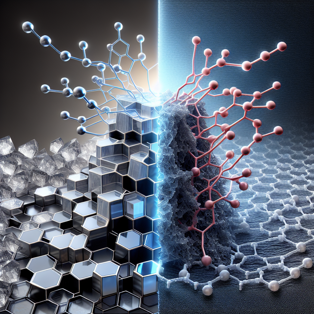
Semiconductor materials are the backbone of modern electronics, enabling the functionality of devices ranging from smartphones to computers. Traditionally, silicon has dominated the semiconductor industry due to its favorable electrical properties, abundance, and well-established manufacturing processes. However, as the demand for faster, smaller, and more efficient electronic components grows, researchers are exploring alternative materials that can overcome the limitations of silicon. One of the most promising candidates is graphene, a single layer of carbon atoms arranged in a two-dimensional lattice. Graphene exhibits exceptional electrical conductivity, mechanical strength, and thermal properties, making it an attractive option for next-generation semiconductor applications. This transition from silicon to graphene represents a significant shift in material science, with the potential to revolutionize the electronics industry and pave the way for innovative technologies.
Advantages of Graphene Over Silicon in Semiconductor Applications
The semiconductor industry has long relied on silicon as the foundational material for electronic devices, owing to its favorable electrical properties and abundance. However, as the demand for faster, smaller, and more efficient devices continues to escalate, researchers are increasingly exploring alternative materials that can surpass the limitations of silicon. Among these alternatives, graphene has emerged as a frontrunner, offering a plethora of advantages that position it as a transformative material in semiconductor applications.
One of the most significant advantages of graphene is its exceptional electrical conductivity. Graphene, a single layer of carbon atoms arranged in a two-dimensional lattice, exhibits electron mobility that is orders of magnitude higher than that of silicon. This property allows for faster electron transport, which can lead to quicker switching speeds in transistors. As a result, devices made from graphene could operate at higher frequencies, enabling advancements in high-speed computing and telecommunications. Furthermore, the high electron mobility of graphene can facilitate the development of low-power devices, as they require less energy to achieve the same performance levels compared to their silicon counterparts.
In addition to its superior electrical properties, graphene also boasts remarkable thermal conductivity. This characteristic is crucial in semiconductor applications, where heat dissipation is a significant concern. Silicon devices often face challenges related to heat buildup, which can lead to performance degradation and reduced lifespan. Graphene’s ability to efficiently conduct heat away from active components can mitigate these issues, allowing for more reliable operation and potentially extending the operational life of electronic devices. Consequently, the integration of graphene into semiconductor technology could pave the way for more robust and durable products.
Moreover, the mechanical strength of graphene is another compelling advantage. Despite being incredibly lightweight, graphene is approximately 200 times stronger than steel. This exceptional strength can enhance the structural integrity of semiconductor devices, making them more resilient to physical stress and environmental factors. As the miniaturization of electronic components continues, the need for materials that can withstand increased mechanical strain becomes paramount. Graphene’s robustness could lead to the development of more durable devices that maintain performance under challenging conditions.
Transitioning from silicon to graphene also opens up new avenues for flexibility in semiconductor design. Graphene can be easily integrated into various substrates, including flexible and transparent materials, which is particularly advantageous for applications in wearable technology and flexible electronics. This adaptability allows for innovative designs that were previously unattainable with traditional silicon-based technologies. As a result, the potential for creating lightweight, bendable devices could revolutionize consumer electronics and expand the possibilities for new applications.
Furthermore, the scalability of graphene production is becoming increasingly feasible, with advancements in synthesis techniques such as chemical vapor deposition and liquid-phase exfoliation. These methods are paving the way for the mass production of high-quality graphene, which is essential for its adoption in commercial semiconductor applications. As production techniques improve, the cost of graphene is expected to decrease, making it a more viable alternative to silicon in the long term.
In conclusion, the transition from silicon to graphene in semiconductor applications presents a multitude of advantages, including superior electrical and thermal conductivity, exceptional mechanical strength, and design flexibility. As research continues to advance and production methods become more efficient, graphene holds the potential to redefine the landscape of semiconductor technology, enabling the development of faster, more efficient, and more durable electronic devices. The future of semiconductors may very well be shaped by this remarkable material, marking a significant shift in the industry.
The Role of Graphene in Next-Generation Electronics
As the demand for faster, smaller, and more efficient electronic devices continues to escalate, the semiconductor industry is undergoing a significant transformation. Traditionally dominated by silicon, the landscape of semiconductor materials is evolving, with graphene emerging as a frontrunner in next-generation electronics. This transition is not merely a shift in materials but represents a fundamental change in how we approach the design and functionality of electronic components.
Graphene, a single layer of carbon atoms arranged in a two-dimensional honeycomb lattice, possesses remarkable electrical, thermal, and mechanical properties. Its exceptional electron mobility, which is significantly higher than that of silicon, allows for faster signal transmission and reduced energy consumption. This characteristic is particularly crucial in high-frequency applications, such as radio frequency identification (RFID) and high-speed transistors, where performance is paramount. As researchers explore the potential of graphene in these areas, the implications for device miniaturization and efficiency become increasingly apparent.
Moreover, the thermal conductivity of graphene is another compelling advantage. In electronic devices, managing heat is critical to maintaining performance and reliability. Graphene’s ability to dissipate heat effectively can lead to more robust designs that can operate at higher power levels without the risk of overheating. This property is especially beneficial in power electronics, where efficiency and thermal management are essential for the longevity and performance of devices.
Transitioning from silicon to graphene also opens up new avenues for flexibility in electronic design. Unlike traditional semiconductor materials, graphene can be integrated into flexible substrates, paving the way for innovative applications in wearable technology and flexible displays. This flexibility not only enhances the user experience but also expands the potential for new product categories that were previously unattainable with rigid materials. As industries increasingly seek to incorporate smart technology into everyday objects, the role of graphene in enabling these advancements cannot be overstated.
Furthermore, the scalability of graphene production is a critical factor in its adoption as a semiconductor material. While challenges remain in terms of large-scale synthesis and integration into existing manufacturing processes, advancements in chemical vapor deposition (CVD) and other fabrication techniques are making it increasingly feasible to produce high-quality graphene at scale. As these methods continue to improve, the cost-effectiveness of graphene-based devices will likely enhance their competitiveness against traditional silicon-based technologies.
In addition to its electrical and thermal properties, graphene’s inherent chemical stability and mechanical strength contribute to its appeal in next-generation electronics. These attributes not only enhance the durability of devices but also enable the development of new functionalities, such as sensors that can operate in harsh environments. The potential for graphene to serve as a platform for multifunctional devices is an exciting prospect that could redefine the capabilities of electronic systems.
In conclusion, the transition from silicon to graphene in semiconductor materials signifies a pivotal moment in the evolution of electronics. With its superior electrical and thermal properties, flexibility, and potential for large-scale production, graphene is poised to play a crucial role in shaping the future of electronic devices. As research and development continue to advance, the integration of graphene into mainstream applications will likely lead to unprecedented innovations, ultimately transforming how we interact with technology in our daily lives. The journey from silicon to graphene is not just a change in materials; it is a leap toward a new era of electronic possibilities.
Challenges in Transitioning from Silicon to Graphene

The transition from silicon to graphene as a primary semiconductor material presents a myriad of challenges that must be addressed to fully realize the potential of graphene in electronic applications. While silicon has dominated the semiconductor industry for decades due to its well-understood properties and established manufacturing processes, graphene offers unique advantages such as high electron mobility, flexibility, and thermal conductivity. However, these benefits come with significant hurdles that researchers and engineers must overcome.
One of the foremost challenges in transitioning to graphene is the difficulty in producing high-quality graphene at scale. Current methods, such as mechanical exfoliation and chemical vapor deposition, often yield graphene with defects or impurities that can adversely affect its electronic properties. The presence of these defects can lead to variability in performance, making it difficult to achieve the consistent quality required for commercial applications. Moreover, scaling up production while maintaining the integrity of the material remains a significant obstacle. As the demand for graphene-based devices increases, developing cost-effective and reliable manufacturing techniques will be crucial.
In addition to production challenges, integrating graphene into existing semiconductor fabrication processes poses another significant hurdle. The semiconductor industry has established a complex ecosystem built around silicon, with a vast array of tools, techniques, and materials optimized for silicon-based devices. Transitioning to graphene requires not only the development of new fabrication methods but also the adaptation of existing processes to accommodate the unique properties of graphene. For instance, the compatibility of graphene with traditional doping techniques, which are essential for creating p-type and n-type semiconductors, is still under investigation. This lack of established methods for doping graphene effectively complicates its integration into current semiconductor technologies.
Furthermore, the electronic band structure of graphene presents challenges that differ from those of silicon. Graphene is a zero-bandgap semiconductor, which means it does not have an energy gap between the valence and conduction bands. This characteristic can lead to difficulties in turning the material off in digital applications, where a clear distinction between on and off states is essential. Researchers are exploring various strategies to engineer a bandgap in graphene, such as chemical functionalization or the creation of graphene-based heterostructures, but these approaches are still in the experimental stage and require further development to be viable for commercial use.
Thermal management is another critical issue that arises with the use of graphene in electronic devices. While graphene exhibits excellent thermal conductivity, the heat dissipation mechanisms in devices utilizing graphene can differ significantly from those in silicon-based devices. This difference necessitates a reevaluation of thermal management strategies to ensure that devices operate efficiently and reliably under varying conditions. The development of effective thermal interfaces and heat spreaders that can leverage graphene’s properties while maintaining compatibility with other materials is an area of ongoing research.
Lastly, the regulatory and standardization landscape for graphene-based technologies is still in its infancy. As the industry moves toward adopting graphene, establishing standards for quality, performance, and safety will be essential to facilitate widespread acceptance and integration into existing systems. Without a clear regulatory framework, the transition from silicon to graphene may face delays and uncertainties that could hinder its potential impact on the semiconductor industry.
In conclusion, while the transition from silicon to graphene holds great promise for the future of electronics, it is fraught with challenges that must be systematically addressed. From production and integration issues to the need for new doping techniques and thermal management strategies, the path forward requires concerted efforts from researchers, engineers, and industry stakeholders to unlock the full potential of graphene as a semiconductor material.
Comparative Analysis of Electrical Properties: Silicon vs. Graphene
The evolution of semiconductor materials has been a pivotal aspect of technological advancement, particularly in the realm of electronics. Traditionally, silicon has dominated the semiconductor landscape due to its favorable electrical properties, abundance, and well-established fabrication techniques. However, as the demand for faster, smaller, and more efficient electronic devices continues to escalate, researchers are increasingly turning their attention to alternative materials, notably graphene. This two-dimensional carbon allotrope has garnered significant interest due to its exceptional electrical properties, which present both opportunities and challenges when compared to silicon.
To begin with, the electrical conductivity of graphene is one of its most remarkable features. Graphene exhibits a carrier mobility that is several orders of magnitude higher than that of silicon. While silicon has a carrier mobility of approximately 1,500 cm²/V·s, graphene can achieve values exceeding 20,000 cm²/V·s under optimal conditions. This superior mobility allows for faster electron transport, which is crucial for high-speed applications. Consequently, devices made from graphene could potentially operate at much higher frequencies than their silicon counterparts, paving the way for advancements in radio frequency and high-speed digital circuits.
Moreover, the intrinsic properties of graphene enable it to maintain high conductivity even at elevated temperatures. In contrast, silicon suffers from increased scattering of charge carriers as temperature rises, leading to a degradation in performance. This thermal stability of graphene not only enhances its reliability in various environments but also opens avenues for applications in high-temperature electronics, where silicon’s limitations become pronounced. Furthermore, the ability of graphene to function effectively in extreme conditions positions it as a viable candidate for next-generation electronic devices.
In addition to conductivity, the band structure of these materials plays a crucial role in their electrical properties. Silicon is a semiconductor with a well-defined bandgap of about 1.1 eV, which allows for effective control of its electrical properties through doping. This bandgap is essential for the operation of transistors, as it enables the modulation of current flow. On the other hand, graphene is a zero-bandgap semiconductor, which presents both advantages and challenges. While the absence of a bandgap allows for continuous electron flow, it complicates the development of devices that require a clear on-off switching mechanism, such as field-effect transistors (FETs). Researchers are actively exploring methods to engineer a bandgap in graphene through various techniques, including chemical doping and the application of strain, to harness its potential in digital applications.
Another critical aspect to consider is the scalability of these materials. Silicon has a well-established infrastructure for large-scale production, which has driven down costs and facilitated widespread adoption. In contrast, while graphene can be produced through several methods, including chemical vapor deposition and liquid-phase exfoliation, achieving uniformity and scalability remains a challenge. The integration of graphene into existing silicon-based technologies also poses hurdles, as compatibility issues can arise during fabrication processes.
In conclusion, while silicon has long been the cornerstone of semiconductor technology, graphene presents a compelling alternative with its superior electrical properties. The comparative analysis reveals that graphene’s high carrier mobility and thermal stability could revolutionize high-speed and high-temperature applications. However, challenges related to its zero-bandgap nature and scalability must be addressed to fully realize its potential. As research continues to advance, the semiconductor landscape may witness a significant transition, with graphene emerging as a formidable contender alongside silicon in the quest for next-generation electronic devices.
Future Trends in Semiconductor Materials: The Rise of Graphene
As the demand for faster, more efficient electronic devices continues to escalate, the semiconductor industry is undergoing a significant transformation, with a notable shift from traditional silicon-based materials to innovative alternatives like graphene. This transition is driven by the limitations of silicon, which, despite its historical dominance, faces challenges in scaling down to meet the needs of modern technology. As devices become smaller and more powerful, the inherent properties of silicon, such as its electron mobility and thermal conductivity, are proving inadequate for next-generation applications. Consequently, researchers and engineers are increasingly turning their attention to graphene, a material that promises to revolutionize the semiconductor landscape.
Graphene, a single layer of carbon atoms arranged in a two-dimensional honeycomb lattice, exhibits remarkable electrical, thermal, and mechanical properties. Its electron mobility is significantly higher than that of silicon, which allows for faster signal transmission and reduced energy consumption. This characteristic is particularly appealing in the context of high-frequency applications, such as radio frequency identification (RFID) and high-speed transistors. Moreover, graphene’s exceptional thermal conductivity enables efficient heat dissipation, a critical factor in maintaining performance and reliability in densely packed electronic circuits.
In addition to its superior electrical properties, graphene is also highly versatile. It can be integrated with other materials to create hybrid structures that leverage the strengths of both components. For instance, combining graphene with silicon can enhance the performance of existing silicon-based devices while paving the way for the development of entirely new architectures. This hybrid approach not only extends the life of silicon technology but also facilitates a smoother transition to graphene-based systems, allowing manufacturers to capitalize on existing infrastructure while exploring innovative designs.
Furthermore, the scalability of graphene production is becoming increasingly viable. While early methods of synthesizing graphene were costly and time-consuming, advancements in chemical vapor deposition (CVD) and liquid-phase exfoliation techniques have significantly improved the feasibility of large-scale production. As these methods continue to evolve, the cost of graphene is expected to decrease, making it a more accessible option for semiconductor applications. This trend is crucial, as the economic viability of new materials often dictates their adoption in commercial products.
As the semiconductor industry embraces graphene, several future trends are emerging. One notable trend is the development of flexible and wearable electronics, where graphene’s lightweight and flexible nature can be fully exploited. These applications require materials that can withstand bending and stretching without compromising performance, and graphene fits this requirement perfectly. Additionally, the rise of Internet of Things (IoT) devices, which demand low-power and high-efficiency components, aligns well with graphene’s capabilities, further driving its adoption.
Moreover, the integration of graphene into photonic devices is gaining traction. Graphene’s unique optical properties enable it to interact with light in ways that silicon cannot, opening up new possibilities for faster data transmission and advanced communication technologies. As researchers continue to explore these applications, the potential for graphene to redefine the semiconductor landscape becomes increasingly apparent.
In conclusion, the transition from silicon to graphene in semiconductor materials is not merely a trend but a necessary evolution driven by the demands of modern technology. With its superior properties, versatility, and improving production methods, graphene is poised to play a pivotal role in shaping the future of electronics. As the industry continues to explore and harness the potential of this remarkable material, we can anticipate a new era of innovation that will redefine the capabilities of electronic devices and systems.
Q&A
1. **Question:** What are the primary advantages of using graphene over silicon in semiconductor applications?
**Answer:** Graphene offers higher electron mobility, better thermal conductivity, flexibility, and the potential for thinner devices, which can lead to faster and more efficient electronic components.
2. **Question:** What challenges are associated with transitioning from silicon to graphene in semiconductor manufacturing?
**Answer:** Challenges include the difficulty in producing high-quality graphene at scale, integrating graphene with existing silicon-based technologies, and developing suitable fabrication techniques for graphene devices.
3. **Question:** How does the bandgap of graphene compare to that of silicon, and why is this significant?
**Answer:** Graphene has no intrinsic bandgap, while silicon has a bandgap of about 1.1 eV. This lack of a bandgap in graphene makes it less suitable for traditional digital logic applications but opens up possibilities for high-frequency and analog applications.
4. **Question:** What potential applications could benefit from the use of graphene in semiconductors?
**Answer:** Potential applications include high-speed transistors, flexible electronics, sensors, photodetectors, and advanced communication devices due to graphene’s superior electrical and thermal properties.
5. **Question:** What research is currently being conducted to facilitate the transition from silicon to graphene in semiconductor technology?
**Answer:** Research focuses on methods for synthesizing high-quality graphene, developing techniques for creating a bandgap in graphene, exploring hybrid materials that combine graphene with other semiconductors, and investigating new device architectures that leverage graphene’s unique properties.
Conclusion
The transition from silicon to graphene in semiconductor materials represents a significant advancement in electronics, driven by graphene’s superior electrical, thermal, and mechanical properties. While silicon has been the cornerstone of the semiconductor industry for decades, limitations in miniaturization and performance have prompted the exploration of graphene as a potential alternative. Graphene’s high carrier mobility, flexibility, and ability to operate at higher frequencies make it an attractive candidate for next-generation devices. However, challenges such as large-scale production, integration with existing technologies, and the development of suitable fabrication techniques must be addressed. In conclusion, while graphene holds great promise for revolutionizing semiconductor technology, further research and innovation are essential to fully realize its potential and facilitate a successful transition from silicon.