“Revolutionizing Connectivity: The Journey of Chip Packaging from Legacy to Advanced Nodes.”
Introduction
The evolution of chip packaging has been a critical aspect of semiconductor technology, reflecting the industry’s shift from legacy systems to advanced nodes. Initially, chip packaging focused on basic protection and connectivity, utilizing simple materials and designs. As the demand for higher performance, miniaturization, and energy efficiency grew, packaging technologies evolved to accommodate complex integrated circuits and multi-chip modules. Innovations such as flip-chip, system-in-package (SiP), and 3D packaging have emerged, enabling greater functionality and reduced form factors. This progression not only enhances electrical performance and thermal management but also supports the rapid advancements in computing power and mobile devices, marking a significant transformation in how chips are designed, manufactured, and integrated into modern electronics.
Historical Overview of Chip Packaging Techniques
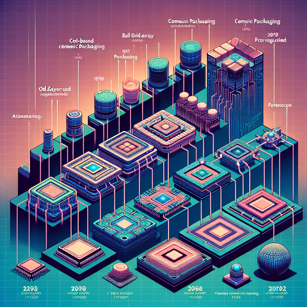
The evolution of chip packaging techniques has been a critical aspect of semiconductor development, reflecting the rapid advancements in technology and the increasing demands for performance, efficiency, and miniaturization. In the early days of semiconductor manufacturing, packaging was a relatively straightforward process, primarily focused on protecting the delicate silicon die from environmental factors while providing electrical connections to the external world. The first packages, such as dual in-line packages (DIPs), were bulky and limited in terms of performance, but they laid the groundwork for future innovations.
As the demand for smaller and more powerful devices grew, the industry began to explore new packaging methods that could accommodate the shrinking size of chips while enhancing their performance. The introduction of surface mount technology (SMT) in the 1980s marked a significant turning point in chip packaging. SMT allowed for components to be mounted directly onto the surface of printed circuit boards, reducing the overall footprint and enabling higher density layouts. This shift not only improved manufacturing efficiency but also facilitated the development of more compact consumer electronics, paving the way for the proliferation of personal computers and mobile devices.
In the 1990s, the advent of ball grid array (BGA) packaging further revolutionized the landscape of chip packaging. BGAs provided a more efficient means of connecting chips to circuit boards, utilizing an array of solder balls instead of traditional pins. This innovation allowed for better thermal performance and electrical characteristics, as well as increased I/O density. As a result, BGAs became the preferred choice for high-performance applications, including graphics processing units (GPUs) and microprocessors, where heat dissipation and signal integrity are paramount.
As technology continued to advance, the industry faced new challenges related to the increasing complexity of integrated circuits. The introduction of flip-chip technology in the late 1990s represented another leap forward in chip packaging. Flip-chip packaging enabled direct electrical connections between the chip and the substrate, eliminating the need for wire bonding and allowing for shorter interconnects. This innovation not only improved electrical performance but also facilitated the integration of multiple functions within a single package, leading to the rise of system-in-package (SiP) solutions. SiP technology has become increasingly important in applications such as smartphones and IoT devices, where space is at a premium and functionality must be maximized.
In recent years, the push towards advanced nodes has driven further innovations in chip packaging. The transition to smaller process nodes, such as 7nm and 5nm technologies, has necessitated the development of advanced packaging techniques that can accommodate the unique challenges posed by these smaller geometries. Techniques such as 3D packaging and chiplet architectures have emerged as viable solutions, allowing for the stacking of multiple dies within a single package. This approach not only enhances performance by reducing interconnect lengths but also enables greater design flexibility and improved yield.
Moreover, the integration of heterogeneous materials and processes has become increasingly prevalent, allowing for the combination of different types of chips—such as analog, digital, and RF components—within a single package. This trend reflects the industry’s ongoing commitment to innovation and adaptability in response to the ever-evolving landscape of semiconductor technology. As we look to the future, it is clear that the historical evolution of chip packaging techniques has set the stage for continued advancements, ensuring that the semiconductor industry remains at the forefront of technological progress.
Key Innovations in Advanced Node Packaging
The evolution of chip packaging has undergone significant transformations, particularly with the advent of advanced nodes that have redefined the landscape of semiconductor technology. As the demand for higher performance, reduced power consumption, and increased functionality continues to rise, innovations in packaging have become crucial in addressing these challenges. One of the key innovations in advanced node packaging is the shift towards three-dimensional (3D) packaging techniques. This approach allows for the stacking of multiple die, which not only saves space but also enhances performance by reducing the distance that signals must travel between components. By integrating various functionalities into a single package, manufacturers can achieve greater efficiency and improved thermal management, which are essential for high-performance applications.
Moreover, the introduction of advanced materials has played a pivotal role in the evolution of chip packaging. Traditional materials such as epoxy resins and silicon have been supplemented with new compounds that offer superior thermal conductivity and electrical performance. For instance, the use of organic substrates has become increasingly prevalent, as they provide a lightweight and flexible alternative to conventional materials. These advancements enable better heat dissipation, which is critical in maintaining the reliability and longevity of semiconductor devices, especially as they operate at higher frequencies and power levels.
In addition to material innovations, the integration of advanced interconnect technologies has significantly impacted chip packaging. The transition from wire bonding to flip-chip technology has allowed for a more compact design and improved electrical performance. Flip-chip packaging facilitates direct connections between the chip and the substrate, minimizing parasitic inductance and capacitance, which are detrimental to high-speed signal integrity. Furthermore, the development of micro-bump technology has enabled finer pitch interconnections, allowing for denser packaging configurations that are essential for modern applications such as mobile devices and high-performance computing.
Another noteworthy innovation is the implementation of system-in-package (SiP) solutions, which combine multiple integrated circuits (ICs) and passive components into a single package. This approach not only reduces the overall footprint but also enhances functionality by enabling heterogeneous integration. SiP technology allows designers to mix and match different technologies, such as analog, digital, and RF components, within a single package, thereby streamlining the design process and improving performance. As a result, SiP has become a preferred choice for applications requiring high levels of integration, such as Internet of Things (IoT) devices and wearable technology.
Furthermore, the rise of advanced packaging techniques such as fan-out wafer-level packaging (FOWLP) has revolutionized the industry by providing a cost-effective solution for high-density applications. FOWLP allows for the redistribution of I/O pads, enabling a larger number of connections in a smaller area. This innovation not only enhances the electrical performance of the device but also simplifies the manufacturing process, making it an attractive option for semiconductor manufacturers looking to optimize production efficiency.
As the semiconductor industry continues to push the boundaries of technology, the importance of advanced node packaging innovations cannot be overstated. These advancements not only address the immediate challenges posed by shrinking geometries and increasing complexity but also pave the way for future developments in chip design and manufacturing. By embracing these innovations, the industry is well-positioned to meet the growing demands for high-performance, energy-efficient, and compact electronic devices, ultimately shaping the future of technology.
Impact of Moore’s Law on Chip Packaging Evolution

The evolution of chip packaging has been significantly influenced by Moore’s Law, which posits that the number of transistors on a microchip doubles approximately every two years, leading to increased performance and reduced costs. This exponential growth in transistor density has necessitated corresponding advancements in chip packaging technologies to accommodate the rising complexity and functionality of integrated circuits. As transistors shrink and become more densely packed, the challenges associated with heat dissipation, signal integrity, and power delivery have become increasingly pronounced, prompting innovations in packaging solutions.
Initially, traditional packaging methods, such as dual in-line packages (DIPs) and surface-mount technology (SMT), were sufficient for the relatively low-density chips of earlier generations. However, as the industry progressed towards smaller geometries, the limitations of these legacy packaging techniques became evident. The need for improved thermal management and electrical performance led to the development of more sophisticated packaging solutions, such as ball grid array (BGA) and chip-on-board (COB) technologies. These advancements allowed for better heat dissipation and enhanced electrical connectivity, which were critical as chip designs evolved to incorporate more transistors and higher frequencies.
Moreover, the transition to advanced nodes has introduced new materials and techniques in chip packaging. For instance, the integration of organic substrates and advanced dielectrics has enabled the production of thinner and lighter packages, which are essential for mobile and portable devices. Additionally, the adoption of 3D packaging technologies, such as through-silicon vias (TSVs) and stacked die configurations, has emerged as a response to the increasing demand for higher performance in a smaller footprint. These innovations not only facilitate greater interconnectivity between chips but also significantly reduce the distance signals must travel, thereby improving overall performance and reducing latency.
As the industry continues to push the boundaries of Moore’s Law, the impact on chip packaging is further amplified by the growing importance of heterogeneous integration. This approach allows for the combination of different types of chips—such as processors, memory, and specialized accelerators—within a single package. Consequently, packaging technologies must evolve to support diverse materials and form factors, ensuring that they can accommodate various thermal and electrical requirements. The rise of system-in-package (SiP) solutions exemplifies this trend, as they enable the integration of multiple functions into a compact form factor, thereby enhancing performance while minimizing space.
In addition to performance considerations, the sustainability of chip packaging has become a focal point in recent years. As the semiconductor industry grapples with environmental concerns, there is a growing emphasis on developing eco-friendly packaging materials and processes. This shift is not only driven by regulatory pressures but also by consumer demand for greener products. Consequently, manufacturers are exploring biodegradable materials and recyclable packaging designs, which align with the broader goals of reducing the environmental impact of electronic waste.
In conclusion, the impact of Moore’s Law on chip packaging evolution is profound and multifaceted. As transistor densities continue to increase, the challenges associated with heat management, signal integrity, and integration complexity necessitate ongoing innovation in packaging technologies. From the early days of simple DIPs to the sophisticated 3D and heterogeneous packaging solutions of today, the journey reflects the semiconductor industry’s relentless pursuit of performance and efficiency. As we look to the future, it is clear that the evolution of chip packaging will remain a critical component in the ongoing advancement of microelectronics, shaping the next generation of devices and applications.
Comparison of Legacy vs. Modern Packaging Materials
The evolution of chip packaging has been a critical aspect of semiconductor technology, reflecting the industry’s relentless pursuit of performance, efficiency, and miniaturization. In this context, a comparison of legacy and modern packaging materials reveals significant advancements that have transformed the landscape of electronic devices. Historically, legacy packaging materials such as ceramic and traditional epoxy resins dominated the market. These materials, while effective in their time, presented limitations in terms of thermal performance, weight, and size. Ceramic packages, for instance, offered excellent thermal conductivity and mechanical stability, making them suitable for high-reliability applications. However, their rigidity and weight often hindered integration into compact consumer electronics, where space and weight constraints are paramount.
As the demand for smaller, more powerful devices grew, the semiconductor industry began to explore alternative materials that could meet the evolving requirements of modern applications. This shift led to the adoption of advanced polymer-based materials, which provided a more flexible and lightweight solution. Modern packaging materials, such as low-k dielectrics and advanced thermoplastics, have emerged as viable alternatives, offering improved electrical performance and reduced signal loss. These materials not only facilitate higher integration densities but also support the miniaturization of components, enabling the development of sophisticated systems-on-chip (SoCs) that are essential for today’s high-performance computing and mobile devices.
Moreover, the transition from legacy to modern packaging materials has been driven by the need for enhanced thermal management. As chip designs have become more complex and power-dense, effective heat dissipation has become a critical concern. Advanced packaging solutions, such as thermal interface materials (TIMs) and heat spreaders made from materials like copper and graphite, have been developed to address these challenges. These innovations allow for better thermal conductivity and heat dissipation, ensuring that modern chips can operate efficiently without overheating. Consequently, the integration of these materials has not only improved the reliability of semiconductor devices but has also extended their operational lifespan.
In addition to thermal performance, the electrical properties of packaging materials have also seen significant advancements. Legacy materials often struggled with issues such as parasitic capacitance and inductance, which could adversely affect signal integrity. In contrast, modern materials are engineered to minimize these effects, allowing for faster signal transmission and improved overall performance. The introduction of materials with lower dielectric constants has been particularly beneficial in high-frequency applications, where maintaining signal integrity is crucial. This shift has enabled the development of high-speed communication devices and advanced computing systems that are essential in today’s data-driven world.
Furthermore, the environmental impact of packaging materials has become an increasingly important consideration in the semiconductor industry. Legacy materials often posed challenges in terms of recyclability and environmental sustainability. In response, manufacturers are now focusing on developing eco-friendly packaging solutions that reduce waste and promote sustainability. Biodegradable polymers and recyclable materials are gaining traction, reflecting a broader industry commitment to minimizing the ecological footprint of semiconductor manufacturing.
In conclusion, the comparison of legacy and modern packaging materials highlights a remarkable evolution driven by the need for enhanced performance, efficiency, and sustainability. As the semiconductor industry continues to innovate, the ongoing development of advanced materials will play a pivotal role in shaping the future of chip packaging, ultimately enabling the next generation of electronic devices that are faster, smaller, and more environmentally friendly. This evolution not only underscores the importance of material science in semiconductor technology but also sets the stage for continued advancements in the field.
Future Trends in Chip Packaging Technology
As the semiconductor industry continues to advance, the evolution of chip packaging technology is becoming increasingly critical to meet the demands of modern electronics. The future of chip packaging is poised to undergo significant transformations, driven by the need for higher performance, greater efficiency, and miniaturization. One of the most prominent trends is the shift towards 3D packaging, which allows for the stacking of multiple chip layers. This approach not only reduces the footprint of devices but also enhances performance by minimizing the distance data must travel between components. As a result, 3D packaging is becoming a preferred solution for applications requiring high bandwidth and low latency, such as artificial intelligence and high-performance computing.
In addition to 3D packaging, the integration of heterogeneous materials is gaining traction. This trend involves combining different types of chips, such as logic, memory, and sensors, into a single package. By leveraging the strengths of various technologies, manufacturers can create more versatile and powerful systems-on-chip (SoCs). This integration not only improves performance but also reduces power consumption, which is a critical factor in mobile and portable devices. As the Internet of Things (IoT) continues to expand, the demand for such integrated solutions will only increase, prompting further innovation in packaging techniques.
Moreover, the rise of advanced packaging technologies, such as fan-out wafer-level packaging (FOWLP) and system-in-package (SiP), is reshaping the landscape of chip design. FOWLP allows for a larger number of I/O connections while maintaining a compact form factor, making it ideal for applications that require high-density interconnections. On the other hand, SiP technology enables the integration of multiple chips within a single package, facilitating the development of multifunctional devices. As these advanced packaging methods become more mainstream, they will enable manufacturers to push the boundaries of what is possible in terms of device performance and functionality.
Another significant trend is the increasing emphasis on sustainability within the semiconductor industry. As environmental concerns grow, manufacturers are exploring eco-friendly materials and processes in chip packaging. This shift not only addresses regulatory pressures but also aligns with consumer preferences for greener products. Innovations such as biodegradable substrates and recyclable packaging materials are being developed to reduce the environmental impact of semiconductor manufacturing. Consequently, sustainability is becoming a key consideration in the design and production of chip packaging, influencing future trends and practices.
Furthermore, the ongoing miniaturization of electronic components necessitates advancements in thermal management solutions. As chips become smaller and more powerful, managing heat dissipation becomes increasingly challenging. Future packaging technologies will need to incorporate advanced thermal management techniques, such as embedded heat spreaders and advanced cooling solutions, to ensure reliable performance. This focus on thermal efficiency will be essential for maintaining the integrity and longevity of high-performance devices.
In conclusion, the future of chip packaging technology is characterized by a convergence of innovative approaches aimed at enhancing performance, efficiency, and sustainability. As the industry embraces 3D packaging, heterogeneous integration, advanced packaging methods, and eco-friendly practices, it is clear that the evolution of chip packaging will play a pivotal role in shaping the next generation of electronic devices. With these advancements, manufacturers will be better equipped to meet the ever-growing demands of consumers and industries alike, paving the way for a more connected and technologically advanced future.
Q&A
1. **Question:** What are legacy chip packaging technologies?
**Answer:** Legacy chip packaging technologies refer to traditional methods such as Dual In-line Package (DIP) and Surface Mount Technology (SMT) that were widely used before the advent of advanced packaging techniques.
2. **Question:** What advancements have been made in chip packaging for advanced nodes?
**Answer:** Advancements include 3D packaging, System-in-Package (SiP), and Chiplet architectures, which enhance performance, reduce power consumption, and improve thermal management.
3. **Question:** How has the demand for miniaturization influenced chip packaging evolution?
**Answer:** The demand for miniaturization has led to the development of smaller, more efficient packaging solutions that allow for higher integration of components and reduced footprint on circuit boards.
4. **Question:** What role does thermal management play in modern chip packaging?
**Answer:** Thermal management is critical in modern chip packaging to dissipate heat effectively, ensuring reliability and performance of high-density and high-performance chips.
5. **Question:** How do advanced packaging techniques impact manufacturing costs?
**Answer:** Advanced packaging techniques can initially increase manufacturing costs due to complexity, but they often lead to cost savings in the long run through improved performance, reduced material usage, and lower power consumption.
Conclusion
The evolution of chip packaging has significantly transformed from traditional legacy methods to advanced nodes, driven by the need for higher performance, miniaturization, and energy efficiency. Innovations in materials, design, and manufacturing processes have enabled the integration of complex functionalities within smaller footprints, enhancing thermal management and electrical performance. As semiconductor technology continues to advance, the future of chip packaging will likely focus on further improving scalability, reliability, and sustainability, ensuring that packaging keeps pace with the demands of next-generation applications in areas such as artificial intelligence, IoT, and high-performance computing.