“3D ICs: Elevating Performance Through Innovative Semiconductor Packaging.”
Introduction
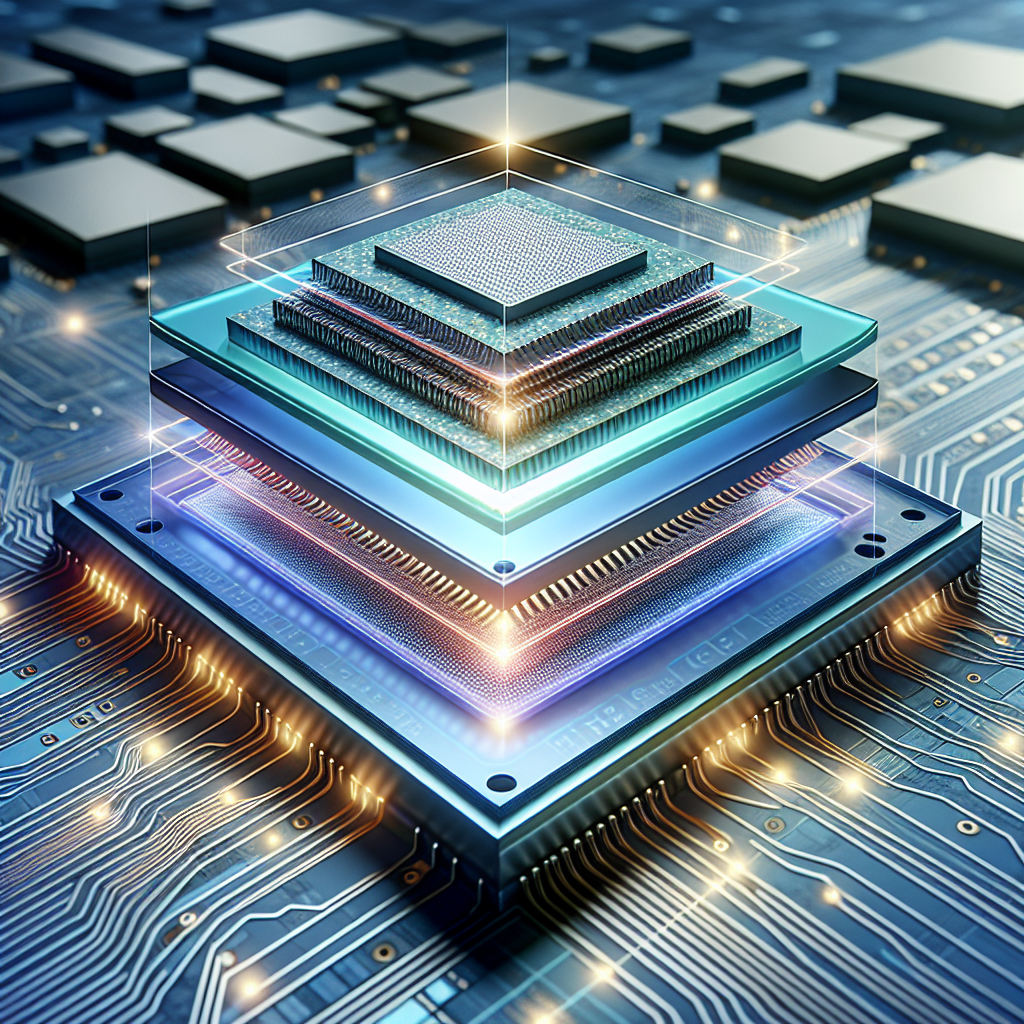
3D Integrated Circuits (3D ICs) represent a transformative advancement in semiconductor packaging technology, enabling the stacking of multiple integrated circuits vertically to enhance performance, reduce power consumption, and minimize footprint. By integrating various functionalities within a compact form factor, 3D ICs facilitate faster data transfer and improved thermal management, addressing the growing demands for higher performance in applications such as high-performance computing, mobile devices, and the Internet of Things (IoT). This innovative approach not only optimizes space but also allows for heterogeneous integration, where different technologies can coexist within a single package, paving the way for more efficient and powerful electronic systems. As the semiconductor industry continues to evolve, 3D ICs are poised to play a crucial role in meeting the challenges of modern computing and connectivity.
Advantages of 3D ICs in Modern Semiconductor Packaging
The advent of three-dimensional integrated circuits (3D ICs) has revolutionized the landscape of semiconductor packaging, offering a multitude of advantages that significantly enhance performance and efficiency. One of the most compelling benefits of 3D IC technology is its ability to dramatically reduce the physical footprint of semiconductor devices. By stacking multiple layers of integrated circuits vertically, manufacturers can achieve higher levels of integration without increasing the overall size of the package. This compact design not only conserves space but also facilitates the development of smaller, more powerful electronic devices, which is particularly crucial in the era of mobile computing and the Internet of Things (IoT).
In addition to space efficiency, 3D ICs provide substantial improvements in interconnectivity. Traditional two-dimensional (2D) ICs often suffer from longer interconnect lengths, which can lead to increased latency and power consumption. In contrast, 3D ICs utilize through-silicon vias (TSVs) and microbumps to create shorter interconnections between stacked layers. This reduction in distance not only enhances signal integrity but also minimizes the time it takes for data to travel between components, resulting in faster processing speeds. Consequently, applications that demand high bandwidth and low latency, such as artificial intelligence and high-performance computing, benefit immensely from the implementation of 3D IC technology.
Moreover, the thermal management capabilities of 3D ICs represent another significant advantage. As devices become more powerful, managing heat dissipation becomes increasingly critical. The vertical stacking of components in 3D ICs allows for more efficient heat distribution and dissipation, as heat can be conducted through the layers more effectively than in traditional packaging. This improved thermal performance not only enhances reliability but also extends the lifespan of semiconductor devices, making them more suitable for demanding applications.
Furthermore, 3D ICs enable heterogeneous integration, which allows for the combination of different technologies and materials within a single package. This flexibility is particularly advantageous in modern semiconductor design, where the integration of diverse functionalities—such as analog, digital, and RF components—can lead to more versatile and capable devices. By leveraging heterogeneous integration, manufacturers can create specialized solutions tailored to specific applications, thereby enhancing performance and reducing time-to-market.
Another noteworthy advantage of 3D ICs is their potential for cost reduction in the long term. While the initial investment in 3D IC technology may be higher due to the complexity of manufacturing processes, the overall cost of ownership can decrease as a result of reduced material usage and improved performance. The ability to integrate multiple functions into a single package can lead to fewer components being required, which not only lowers material costs but also simplifies assembly and reduces the likelihood of defects.
In conclusion, the advantages of 3D ICs in modern semiconductor packaging are manifold, encompassing improved space efficiency, enhanced interconnectivity, superior thermal management, heterogeneous integration, and potential cost savings. As the demand for high-performance, compact electronic devices continues to grow, the adoption of 3D IC technology is poised to play a pivotal role in shaping the future of semiconductor design and manufacturing. By unlocking higher performance capabilities, 3D ICs are not only meeting the challenges of contemporary applications but also paving the way for innovations that will define the next generation of electronic systems.
Key Technologies Driving 3D IC Development
The evolution of semiconductor technology has reached a pivotal moment with the advent of 3D integrated circuits (ICs), which promise to significantly enhance performance and efficiency in electronic devices. Central to this advancement are several key technologies that are driving the development of 3D ICs, each contributing to the overall capability and functionality of these sophisticated systems. As the demand for higher performance in computing and communication continues to escalate, understanding these technologies becomes essential for grasping the future landscape of semiconductor packaging.
One of the most critical technologies underpinning 3D IC development is through-silicon vias (TSVs). TSVs facilitate vertical interconnections between different layers of silicon, allowing for a compact design that minimizes the distance signals must travel. This reduction in distance not only enhances speed but also decreases power consumption, which is a crucial factor in modern electronics. By enabling multiple layers of circuitry to be stacked, TSVs effectively increase the density of components, leading to improved performance without a corresponding increase in footprint. As a result, TSV technology is a cornerstone of 3D IC architecture, enabling manufacturers to create more powerful and efficient devices.
In addition to TSVs, micro-bumping technology plays a vital role in the assembly of 3D ICs. Micro-bumps are tiny solder bumps that connect the various layers of silicon wafers, ensuring reliable electrical connections while maintaining a low profile. This technology allows for finer pitch connections, which is essential for achieving the high-density interconnects required in 3D ICs. Furthermore, the use of micro-bumps enhances thermal management, as they can be designed to dissipate heat more effectively than traditional solder joints. Consequently, micro-bumping technology not only supports the structural integrity of 3D ICs but also contributes to their overall performance by addressing thermal challenges.
Another significant technology driving the development of 3D ICs is advanced packaging techniques, such as fan-out wafer-level packaging (FOWLP). FOWLP allows for the integration of multiple chips into a single package, providing a more efficient use of space and resources. This technique enables the creation of larger, more complex systems on a chip (SoCs) that can incorporate various functionalities, such as processing, memory, and connectivity, all within a compact form factor. By leveraging FOWLP, manufacturers can achieve higher performance levels while also reducing the overall size and weight of electronic devices, which is particularly advantageous in mobile and portable applications.
Moreover, the integration of heterogeneous materials and components is another key aspect of 3D IC technology. The ability to combine different types of chips, such as analog, digital, and RF components, into a single 3D package allows for greater design flexibility and optimization. This heterogeneous integration not only enhances performance but also enables the development of specialized applications tailored to specific market needs. As industries increasingly demand customized solutions, the ability to integrate diverse technologies within a single package becomes a significant competitive advantage.
In conclusion, the development of 3D ICs is being propelled by a confluence of advanced technologies, including TSVs, micro-bumping, FOWLP, and heterogeneous integration. Each of these technologies plays a crucial role in enhancing the performance, efficiency, and versatility of semiconductor packaging. As the industry continues to innovate and refine these technologies, the potential for 3D ICs to revolutionize electronic devices becomes increasingly apparent, paving the way for a new era of high-performance computing and communication solutions.
Challenges in Implementing 3D ICs for High-Performance Applications

The implementation of 3D integrated circuits (ICs) in high-performance applications presents a myriad of challenges that must be addressed to fully realize their potential. As the demand for increased performance, reduced power consumption, and compact form factors continues to rise, the semiconductor industry is increasingly turning to 3D IC technology. However, the transition from traditional 2D designs to 3D architectures is fraught with complexities that can hinder widespread adoption.
One of the primary challenges in implementing 3D ICs is the thermal management of densely packed components. In a 3D IC, multiple layers of active devices are stacked vertically, which can lead to significant heat generation. The close proximity of these layers complicates heat dissipation, as traditional cooling methods may not be effective in such confined spaces. Consequently, innovative thermal management solutions, such as advanced heat spreaders or microfluidic cooling systems, must be developed to ensure that the temperature remains within operational limits. Without effective thermal management, the reliability and performance of 3D ICs can be severely compromised.
In addition to thermal issues, the manufacturing processes for 3D ICs are inherently more complex than those for their 2D counterparts. The integration of multiple layers requires precise alignment and bonding techniques, which can introduce variability and defects during production. Techniques such as through-silicon vias (TSVs) are commonly employed to establish electrical connections between layers, but the fabrication of TSVs adds another layer of complexity to the manufacturing process. Ensuring high yield and low defect rates in 3D IC production is critical, as even minor imperfections can lead to significant performance degradation or complete failure of the device.
Moreover, the design and verification of 3D ICs pose unique challenges. The traditional design flow for 2D ICs may not be directly applicable to 3D architectures, necessitating the development of new design tools and methodologies. Designers must consider not only the individual layers but also the interactions between them, which can complicate the design process. Additionally, verification becomes more challenging as the number of layers increases, requiring advanced simulation techniques to ensure that the final product meets performance specifications. This complexity can lead to longer design cycles and increased costs, which may deter some companies from pursuing 3D IC technology.
Another significant hurdle is the integration of heterogeneous materials and components within a single 3D IC. The ability to combine different types of devices, such as analog, digital, and RF components, can enhance performance and functionality. However, the differing thermal and electrical properties of these materials can lead to compatibility issues, complicating the design and manufacturing processes. Addressing these challenges requires a deep understanding of material science and engineering, as well as innovative approaches to integration.
Finally, the economic factors associated with 3D IC implementation cannot be overlooked. The initial investment in research, development, and manufacturing infrastructure can be substantial. Companies must weigh the potential performance benefits against the costs of transitioning to 3D IC technology. As the market for high-performance applications continues to grow, it is essential for stakeholders to collaborate and share knowledge to overcome these challenges. By addressing thermal management, manufacturing complexities, design verification, material integration, and economic considerations, the semiconductor industry can unlock the full potential of 3D ICs, paving the way for a new era of high-performance applications.
Future Trends in 3D IC Packaging Solutions
As the semiconductor industry continues to evolve, the demand for higher performance, increased functionality, and reduced power consumption drives innovation in packaging solutions. Among the most promising advancements is the development of three-dimensional integrated circuits (3D ICs), which offer a transformative approach to semiconductor packaging. Looking ahead, several future trends in 3D IC packaging solutions are poised to reshape the landscape of electronics, enabling more efficient designs and enhanced performance.
One of the most significant trends is the increasing adoption of advanced packaging technologies that facilitate the integration of heterogeneous components. As applications become more complex, the need for diverse functionalities within a single package becomes paramount. 3D ICs allow for the stacking of different types of chips, such as logic, memory, and sensors, thereby optimizing space and improving performance. This heterogeneous integration not only enhances the overall functionality of devices but also reduces the interconnect length, leading to lower latency and improved power efficiency. Consequently, industries such as telecommunications, automotive, and consumer electronics are likely to see a surge in the implementation of 3D ICs to meet their specific performance requirements.
Moreover, the miniaturization of electronic devices continues to be a driving force behind the evolution of 3D IC packaging. As consumer demand for smaller, more powerful devices grows, manufacturers are compelled to explore innovative packaging solutions that can accommodate this trend. 3D ICs inherently support a compact design by stacking chips vertically, which significantly reduces the footprint of the overall package. This miniaturization not only allows for more efficient use of space but also contributes to the reduction of material costs and waste, aligning with the industry’s increasing focus on sustainability. As a result, we can expect to see a broader acceptance of 3D IC technology across various sectors, particularly in mobile devices and wearables.
In addition to miniaturization, the integration of advanced thermal management solutions is becoming increasingly critical in 3D IC packaging. As devices become more powerful, managing heat dissipation effectively is essential to maintain performance and reliability. Future trends indicate a growing emphasis on innovative thermal management techniques, such as microfluidic cooling and advanced heat spreaders, which can be integrated into 3D IC designs. These solutions not only enhance thermal performance but also contribute to the longevity of the devices, making them more appealing to manufacturers and consumers alike.
Furthermore, the rise of artificial intelligence (AI) and machine learning (ML) applications is driving the need for specialized 3D IC packaging solutions. As these technologies require significant computational power and memory bandwidth, traditional packaging methods may struggle to meet the demands. 3D ICs can provide the necessary architecture to support high-performance computing tasks by enabling faster data transfer rates and improved bandwidth. Consequently, we can anticipate a surge in the development of tailored 3D IC solutions specifically designed for AI and ML applications, further solidifying their role in the future of semiconductor packaging.
Lastly, the ongoing advancements in manufacturing processes, such as wafer-level packaging and through-silicon vias (TSVs), are expected to enhance the scalability and cost-effectiveness of 3D ICs. As these technologies mature, they will enable manufacturers to produce 3D ICs at a lower cost and with greater efficiency, making them more accessible to a wider range of applications. This democratization of technology will likely accelerate the adoption of 3D ICs across various industries, paving the way for innovative products and solutions that were previously unattainable.
In conclusion, the future of 3D IC packaging solutions is bright, characterized by trends that emphasize heterogeneous integration, miniaturization, advanced thermal management, and specialized applications. As these trends continue to unfold, they will undoubtedly unlock new levels of performance and efficiency in semiconductor packaging, driving the next wave of innovation in the electronics industry.
Case Studies: Successful Applications of 3D ICs in Industry
The advent of three-dimensional integrated circuits (3D ICs) has revolutionized the semiconductor industry, enabling unprecedented levels of performance and efficiency in various applications. As industries increasingly demand higher performance, lower power consumption, and reduced form factors, 3D ICs have emerged as a compelling solution. Several case studies illustrate the successful implementation of 3D IC technology across different sectors, showcasing its transformative potential.
One notable example can be found in the realm of high-performance computing (HPC). Companies like Intel have leveraged 3D IC technology to enhance the performance of their processors. By stacking multiple layers of silicon dies, Intel has been able to significantly increase the density of transistors while minimizing the distance that signals must travel. This reduction in interconnect length not only boosts speed but also decreases power consumption, which is critical in data centers where energy efficiency is paramount. The introduction of Intel’s 3D packaging technology has allowed for the development of processors that can handle more complex computations, thereby meeting the growing demands of artificial intelligence and machine learning applications.
In the consumer electronics sector, the use of 3D ICs has also gained traction, particularly in mobile devices. For instance, companies like Apple have adopted 3D IC technology in their latest smartphones to enhance performance while maintaining a sleek design. By integrating memory and processing units into a single package, Apple has achieved significant improvements in data transfer rates and energy efficiency. This integration not only allows for faster app loading times and improved multitasking capabilities but also contributes to a longer battery life, which is a critical factor for consumer satisfaction. The success of this approach has set a new standard in the industry, prompting other manufacturers to explore similar 3D packaging solutions.
Moreover, the automotive industry has begun to recognize the advantages of 3D ICs, particularly in the development of advanced driver-assistance systems (ADAS) and autonomous vehicles. Companies like NVIDIA have utilized 3D IC technology to create powerful computing platforms that can process vast amounts of data from sensors in real-time. By stacking multiple processing units, NVIDIA has been able to enhance the computational capabilities of their systems while reducing the physical footprint. This capability is essential for the implementation of complex algorithms that enable features such as object detection, lane-keeping assistance, and adaptive cruise control. As the automotive sector continues to evolve towards greater automation, the role of 3D ICs will likely become even more critical.
In the field of telecommunications, 3D ICs have also made significant strides, particularly in the development of 5G technology. Companies like Qualcomm have embraced 3D packaging to create more efficient radio frequency (RF) components that are essential for high-speed data transmission. By stacking RF front-end modules, Qualcomm has been able to reduce signal loss and improve overall performance, which is vital for meeting the demands of next-generation wireless networks. This innovation not only enhances the user experience but also supports the growing ecosystem of connected devices that rely on robust and reliable communication.
In conclusion, the successful applications of 3D ICs across various industries underscore their potential to unlock higher performance in semiconductor packaging. From high-performance computing and consumer electronics to automotive and telecommunications, the benefits of 3D IC technology are evident. As industries continue to evolve and demand more from their electronic components, the adoption of 3D ICs is likely to expand, paving the way for even more innovative solutions in the future.
Q&A
1. **What are 3D ICs?**
3D ICs (Three-Dimensional Integrated Circuits) are semiconductor devices that stack multiple layers of integrated circuits vertically, allowing for higher density, improved performance, and reduced interconnect lengths.
2. **What are the main advantages of 3D IC technology?**
The main advantages include increased performance due to shorter interconnects, reduced power consumption, enhanced functionality by integrating different technologies, and improved thermal management.
3. **How do 3D ICs impact semiconductor packaging?**
3D ICs enable more compact packaging solutions, allowing for smaller form factors while maintaining or enhancing performance, which is crucial for applications in mobile devices, high-performance computing, and IoT.
4. **What are the challenges associated with 3D ICs?**
Challenges include complex manufacturing processes, thermal management issues, potential reliability concerns due to stacking, and the need for advanced design tools and methodologies.
5. **What applications benefit most from 3D IC technology?**
Applications that benefit include high-performance computing, data centers, mobile devices, artificial intelligence, and advanced telecommunications, where performance and efficiency are critical.
Conclusion
3D ICs represent a significant advancement in semiconductor packaging, enabling higher performance through improved integration, reduced latency, and enhanced power efficiency. By stacking multiple layers of integrated circuits, 3D ICs facilitate shorter interconnects and greater functionality within a smaller footprint. This technology not only addresses the limitations of traditional 2D packaging but also supports the growing demand for compact, high-performance devices in various applications, including computing, telecommunications, and consumer electronics. As the industry continues to innovate, 3D ICs are poised to play a crucial role in the future of semiconductor technology, driving advancements in performance and efficiency.